Configuration Pin Microcontroller AT89S51AT89S51 microcontroller pin arrangement shown in Figure 1.
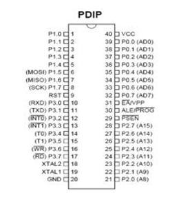 Figure 1. Pin Configuration AT89s515. Functionality of Each Pin Microcontroller AT89S51Microcontroller AT89S51 has pins numbered 40 and generally packaged in DIP (Dual Inline Package). Each pin on the microcontroller AT89S51 have utility as follows:Port 0Port 0 is a function of two ports are on pins 32-39 of AT89S51. In the design of a simple system of this port as the port I / O versatile. For more complex designs involving this pathway dimultiplek external memory to the data bus and address bus.Port 1Port 1 is reserved as I / O ports and are on pins 1-8. Some pins on this port have special functions ie P1.5 (MOSI), P1.6 (MISO), P1.7 (SCK) is used to track the download program.Port 2Port 2 (pins 21-28) is a dual function as a port I / O versatile, or
as high-byte address bus for design involving external memory.Port 3Port 3 is a two-port pin functions are at 10-17, this port has multiple functions, such as those found in table 1.1 below:ALTERNATE ADDRESS BIT BIT NAME FUNCTIONB0h P3.0 RXD Receive Data for serial portB1h P3.1 TXD Transmit Data for serial portB2h P3.2 INT0 External interrupt 0B3H P3.3 INT1 External interrupt 1B4h P3.4 T0 Timer / counter 0 external inputB5h P3.5 T1 Timer / counter 1 external inputP3.6 WR B6h External Data memory write strobeP3.7 RD B7h External Data memory read strobePSEN (Program Store Enable)Is
an output signal that is contained in the pin 29. Its function is as a
control signal to allow a microcontroller to read the program (code) of
the external memory. Normally this pin is connected to pin EPROM. If the execution of the program from the internal ROM or flash memory (ATMEL AT89Sxx), then it is in the off state (high).ALE (Address Latch Enable)ALE
output signal which is at pin 30, the same function with ALE in
microprocessor INTEL 8085, 8088 or 8086. ALE signal is used to
demultiplek address bus and a data bus. ALE signal generate pulses at 1/6 the oscillator frequency and can be used as a clock that can be used in general.EA (External Access)Input signals are on pins 31 which can be given a logic low (ground) or logic high (+ 5V). If given the high logic microcontroller will access the program from the internal ROM (EPROM / flash memory). If given a logic low, the microcontroller will access the program from an external memory.RST (Reset)Reset input on pin 9 is the master reset for AT89S51. Pulse transition from high to low during the second cycle will reset the microcontroller.OscillatorProvided on chip oscillator driven by XTAL connected to pin 18 and pin 19. Necessary stabilizing capacitor of 30 pF. Great value XTAL about 3 MHz to 33 MHz. XTAL1
is the input to a reversal of the oscillator amplifier (inverting
oscillator amplifier) and input to the internal clock operating
circuit. While XTAL2 is the output of the oscillator amplifier reversal.PowerAT89s51 operated at a supply voltage of + 5V, Vcc pin is at number 40 and the Vss (ground) at pin 20.
Figure 1. Pin Configuration AT89s515. Functionality of Each Pin Microcontroller AT89S51Microcontroller AT89S51 has pins numbered 40 and generally packaged in DIP (Dual Inline Package). Each pin on the microcontroller AT89S51 have utility as follows:Port 0Port 0 is a function of two ports are on pins 32-39 of AT89S51. In the design of a simple system of this port as the port I / O versatile. For more complex designs involving this pathway dimultiplek external memory to the data bus and address bus.Port 1Port 1 is reserved as I / O ports and are on pins 1-8. Some pins on this port have special functions ie P1.5 (MOSI), P1.6 (MISO), P1.7 (SCK) is used to track the download program.Port 2Port 2 (pins 21-28) is a dual function as a port I / O versatile, or
as high-byte address bus for design involving external memory.Port 3Port 3 is a two-port pin functions are at 10-17, this port has multiple functions, such as those found in table 1.1 below:ALTERNATE ADDRESS BIT BIT NAME FUNCTIONB0h P3.0 RXD Receive Data for serial portB1h P3.1 TXD Transmit Data for serial portB2h P3.2 INT0 External interrupt 0B3H P3.3 INT1 External interrupt 1B4h P3.4 T0 Timer / counter 0 external inputB5h P3.5 T1 Timer / counter 1 external inputP3.6 WR B6h External Data memory write strobeP3.7 RD B7h External Data memory read strobePSEN (Program Store Enable)Is
an output signal that is contained in the pin 29. Its function is as a
control signal to allow a microcontroller to read the program (code) of
the external memory. Normally this pin is connected to pin EPROM. If the execution of the program from the internal ROM or flash memory (ATMEL AT89Sxx), then it is in the off state (high).ALE (Address Latch Enable)ALE
output signal which is at pin 30, the same function with ALE in
microprocessor INTEL 8085, 8088 or 8086. ALE signal is used to
demultiplek address bus and a data bus. ALE signal generate pulses at 1/6 the oscillator frequency and can be used as a clock that can be used in general.EA (External Access)Input signals are on pins 31 which can be given a logic low (ground) or logic high (+ 5V). If given the high logic microcontroller will access the program from the internal ROM (EPROM / flash memory). If given a logic low, the microcontroller will access the program from an external memory.RST (Reset)Reset input on pin 9 is the master reset for AT89S51. Pulse transition from high to low during the second cycle will reset the microcontroller.OscillatorProvided on chip oscillator driven by XTAL connected to pin 18 and pin 19. Necessary stabilizing capacitor of 30 pF. Great value XTAL about 3 MHz to 33 MHz. XTAL1
is the input to a reversal of the oscillator amplifier (inverting
oscillator amplifier) and input to the internal clock operating
circuit. While XTAL2 is the output of the oscillator amplifier reversal.PowerAT89s51 operated at a supply voltage of + 5V, Vcc pin is at number 40 and the Vss (ground) at pin 20.
No comments:
Post a Comment